| Micro Connector for High Packaging Density Fabricated by Using UV Thick Photoresist |
Toshinori Unno, Toshiyuki Toriyama*, Mohammed Moinul Islam Bhuiyan, Yoshihiko Yokoyama and Susumu Sugiyama
(Ritsumeikan University, *New Energy and Industrial Technology Development Organization )
Keywords: micro connector, thick photoresist, high packaging density, contact resistance.
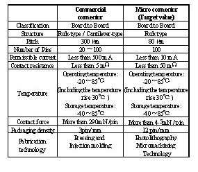
Å@Å@Recently, miniature, light and high functional electronic devices have been developed using high functional LSIs called SOC (system on chip). Miniature connectors with smaller pitches have been required in order to satisfy specifications of these electronic devices. At present, the minimum pitch of commercial connectors is 300 mm, and the manufacturing method is pressing and injection molding. It is difficult to make connectors with pitch smaller than 300 mm by using the pressing and injection molding. The pressing and injection molding are not compatible with high-density packaging, which is required in the advanced IT (Information Technology) market. Table 1 shows the comparison between specification of the commercial connector and that of the present micro connector.
Table 1. Comparison of micro connector with commercial connector having minimum pitch.
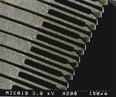
Å@Å@This study focuses on fabrication of micro connectors by combining UV thick resist photolithography and Ni electroforming. This fabrication method is expected to realize high precision micro connectors and high packaging density in mass production. A fork-type micro connector with high aspect ratio and high packaging density was fabricated using UV thick photoresist and Ni electroforming. A negative photoresist (THB-130N) was used as a mold of Ni electroforming. The tips of socket terminal of the micro connector were formed as movable portions using Cu sacrificial layer etching. In order to make firm contact of the micro connector, two-step guidance was adopted. The size of the terminal of fabricated micro connector was 50 mm- thickness and 15 mm-width (minimum). The maximum aspect ratio of the fabricated micro connector is 3.3 and the terminal pitch is 80 mm. Figure 1 shows SEM photograph of the socket terminal which was formed by the Ni electroforming. A contact resistance of a 50 mW,a contact force of 2.08mN,YoungÅfs modulus of 80 GPa and a permissible current of 400 mA (single pair of the plug and socket terminals) were obtained practicl use for the micro connector.
Å@Å@These results show one prospect for development of a micro connector with high - package density, which can be used in next generation of IT market.
Figure 1. SEM photograph of socket terminal by Ni.
Å@
Å@
Å@
Å@