| |
|
|
| |
|
|
| |
| |
|
|
| |
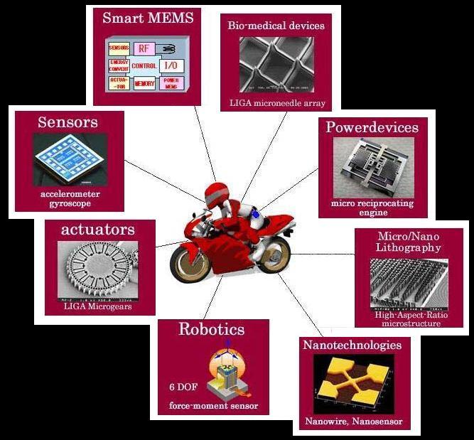
Advent in 1980s, MEMS(micro-electromechanical Systems)
has been under research and development at various Universities
and enterprises throughout the world. To meet present industrial
requirements, RIMST(Research Institute for Microsystem Technology)
in Ritsumeikan University is combining designs, micro-fabrication
and material evaluation by establishing microprocess equipment
at Microsystem center and Synchrotron Radiation light source at
SR center. Under the activities assigned for RIMST, Micro Nano
Integrated Device Lab. consists of research on Micro/Nano Science
Integrated System as 21st century COE program by the ministry
of Education, Culture, Sports, Science and Technology.
Research
at Micro Nano Intergrated Devices Lab. is mainly about MEMS devices
and LIGA. From Integrated Circuit(IC) technology to micromachining
technology, mechanical and electrical systems are combined. Sensors
and Actuators are sensing and driving parts of MEMS devices. The
development of microprocess technology and fabricating microdevices
are our works.
The
output of MEMS is to create intelligent microdevices that can
process or transduce energy from physical, mechanical, optical,
chemical and biological forms as inputs, using microfabrication
techniques expanding from IC technology. Our research group is
archieving many practical results for sensors, actuators, and
process technology by the colaboration with industries.
|
|
| |
|
|
| |
|
|
| |
\
|
|
|
|
|
|
|
|
|
|
|
|
|
|
|
Laser
3D fabrication
|
Excimer
Laser applications
|
Piezoelectric
mirror devices
|
Electrostatic
mirror devices |
|
|
|
|
|
|
| |
Ni-Fe
ELECTROPLATING TECHNOLOGY
|
|
| |
LIGA
(Lithographic Galvonoformung Abformung) process is an effective technology
for reaching high-aspect ratio micro/nano structure. By exposing Synchrotron
Radiation to the resist through X-ray mask, the resist will be shaped
by X-ray lithography. Micromold will be formed by electroplating metals.
The mold will finally be used for batch fabrication of plastic, ceramics
or other materials of micro/nano structure.
|
|
| |
|
|
| |
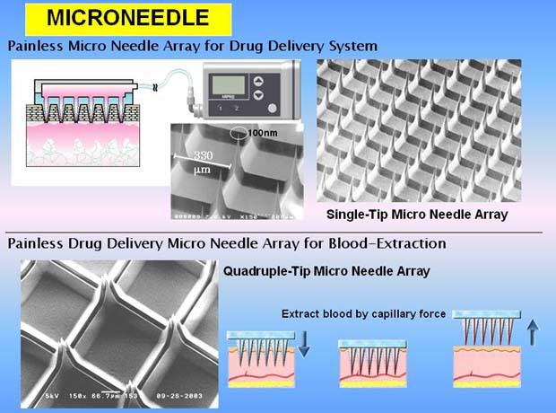
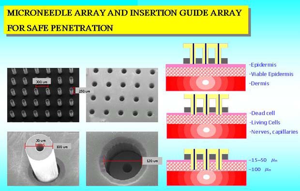
Partly
LIGA processing, microneedle array with a novel 3-D shape
was fabricated. PCT (Plain-pattern to Cross-section Trsansfer)
Technique has been introduced by our research institute.
The 2-D pattern on X-ray mask transfers to 3-D structure
on PMMA. Tip size can be reduced by tilting mask-angle.
The optimized tilting angle has been investigated to reach
nanoscaled actual tip-size. Biomedical application is
our aim of making the microneedle. The needles is developed
for both by drug delivery system and blood extraction
system.The improvement of microneedle shape has been done
with several mask patterns. |
|
Without
fabrication of holes, alternative method of utilizing
microneedle as for blood extraction system has been investigated.
By the capillary force, microneedle with quadruple-tips
can be inserted through skin. Molding process by electroplating
is also employed, known as LIGA process.
|
|
|
|
| |
|
|
| |
In this work, fabrication of electrostatic microactuators as an
application of the LIGA process has been investigated by using
a compact synchrotron radiation source "AURORA". So
far, there are many reports about microactuators fabricated by
surfacemicromachining. The height of the microactuators is limited
to about 1 to 10 micrometer in surfacemicromachining. However,
the LIGA process can fabricate high aspect ratio microactuators
with height of more than 100 micrometer.
The
roughness of sidewalls is an important factor for the performance
of high aspect ratio microstructures. The sidewall roughness of
the Ni microstructure was measured by atomic force microscope
(AFM). The peak to valley in the measurement area was 651 nanometer,
which was equal to the roughness of the absorber sidewall. The
vertical average roughness of the sidewall was 23.1 nanometer.
It can be considered as the real finish roughness of the deep
X-ray lithography.
|
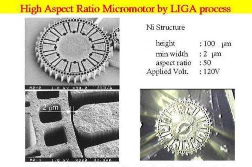
The
structure of microactuator composed of 100 micrometer high Ni
microstructures, a seed layer for electroforming, an isolation
layer of 3 micrometer thick SiO2, and a Si wafer. The Ni microstructures
act a movable electrode, fixed electrodes, a spring beam and
an anchor portion. The movable electrode is separated from the
substrate by sacrificial layer etching of the SiO2. SEM photo(upper)
shows a wobble motor with 1 millimeter diameter, 100 micrometer
height, 2 micrometer minimum width and gap, and then maximum
aspect ratio of 50 after Ni electroforming. These
microactuators can be applied to high accuracy positioning actuators
|
|
|
| |
|
|
| |
|
Using the same technique as microneedle array, PMMA microlens array
having free curved surface has been fabricated ny PCT process. The
diameter of each lens is 5 microns to 1mm. Shape of lens is non
spherical surfaces. Pitch between each lens is 5 mm. The array is
on the maximum chip size of 3 mm. |

|
|
| |
PIEZOELECTRIC
DEVICE APPLICATIONS |
|
| |
Recently,
a miniaturization and highly efficient actuators are progressing
in various fields. In the field of the fluidic systems at present,
the miniaturization of systems is useful for bio-MEMS applications.
In this research, the aim is developing the micro valve used for
a small measurement system which the volumn of air control is
needed. There are various types of actuators currently used for
the microvalves. A Bimorph shape memory alloy is used in order
to open and close the valve by overheating and cooling. The low
frequency is required. Usually the electromagnetic actuator is
giving a large distance in each response but piezoelectric actuator
has a quick response and is easy to miniaturize. Therefore, design
and development of the micro valve using bimorph PZT actuator
is performed. The piezoelectric ceramic is expanded by applied
voltage. The 2 layers of piezoelectric ceramics made the direction
of polarization reversible. After the calculation using the theory
of Bernouilli's equation as a regular flow of incompressibility
and non-viscosity fluid, the experiment value at 98% of the theoretical
value was obtained.
|
|
|
|
| |
MICROGYROSCOPE |
|
| |
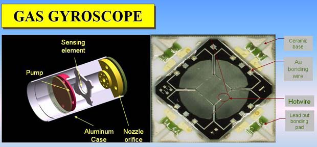
The development
of a dual axis gas gyroscope whose working principle based on
the thermo-resistive effect of silicon-hotwire is presented. The
proposed gas gyroscope has no moving mass, therefore it can eliminate
the inherent problems which usually occur in vibrating gyroscopes.
The sensor configuration consists of a piezoelectric pump and
a micro thermal sensing element, packaged in an aluminum case
with diameter and length of 14mm and 25mm, respectively. The micro
sensing element is formed by four silicon thermistor wires, each
has dimension of 400?4?2?m3, (L?W?T), are arranged in a square-frame
shape. Neon is used for the gas flow inside the sensor case, since
it is an inert gas with high thermal conductivity. The sensing
element has been fabricated from SOI (silicon on insulator) wafer
by conventional MEMS processes. The gyroscope was calibrated by
using a turntable, and the measured sensitivity was 0.15mV/deg/sec,
which is 62 times larger than that of the gas gyroscope with the
same design but using tungsten as sensing element. |

| The
structure of the micro gyroscope is shown in figure above. The
micro gyroscope consists of a cross-shaped and folded silicon
beam with p-type Si piezoresistors, and pillars at the center
and both sides of the beam. The cross-shaped and folded silicon
beam is 50 mm - wide and 50 mm- thick. These piezoresistors are
formed at the locations where the maximum compressive and tensile
stresses are applied. The
design of the micro gyroscope is based on the Coriolis effect.
The micro gyroscope uses the rotary movement of pillars induced
by the four electromagnetic actuators. When the angular rate is
applied to the micro gyroscope, the Coriolis force changes the
stress in the beam. The micro gyroscope detects the change of
stress in the beam via the piezoresistors. The influence of acceleration
can be removed by the combination of the configuration of both
side pillars and thb bridge circuit.
|
|
| |
|
|
|
| |
|
|
| |
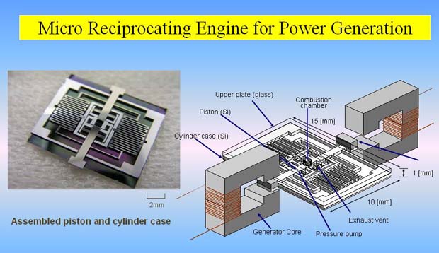
A resonant micro reciprocating engine was designed for electric
power generation. Adopting hydrogen gas as a fuel and silicon
as a structural material, the theoretical electric power was found
to be about 40mW under the conditions that compression ratio is
5, the maximum combustion temperature is 850K, and natural frequency
of the piston-spring system is 610Hz. The fabrication process
based on ICP-RIE bulk micromachining for micro engine was established
and classified into two items: piston and cylinder case(I), packaging
of piston and cylinder case and top glass plate(II). The engine
operation was demonstrated based on air cycle.
|
|
|
|
| |
|
|
| |
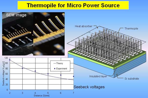
|
A thermopile without a membrane and having self-standing structure
is proposed in
order to realize ideal higher thermal isolation. The proposed
structure has two advantages; the absorbed heat transfers from
hot contacts to cold contacts only through the thermopile and
no heat transfer will occur between the hot and cold contacts,
and the heat absorber area can be increased more than the chip
area. As a consequence, temperature difference between the hot
and cold contacts approaches the ideal value. In this paper, design,
fabrication and characteristics of the self-standing polysilicon-metal
junction thermopile for an accessory micro power generator are
reported, especially focusing on the first advantage.
The
thermocouple is composed of an n - type polysilicon and an Au
junction. The thermopile was fabricated by MICS (Micromachine
Integrated Chip Service: three polysilicon layer structure) organized
by the Cooperative Research Committee for Standardization of Micromachines
in IEE of Japan. |
|
The
experimental results of the Seebeck voltage of the thermopile
(N =10 thermocouples). A black body plate having uniform
typical human skin temperature (307K) was used as the
radiation source. Seebeck voltage of more than 6.2mV was
obtained. The experimental results are in reasonable agreement
with the theoretical calculation. The prospect for application
of the thermopile to an accessory micro power generator
was shown. In future work, a thermopile with an upper
heat absorber will be fabricated and characterized. |
|
|
|
|
| |
|
|
| |
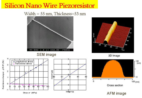
Silicon
nano wires have been studied from the viewpoint of a mechanical
sensor application. Polycrystalline silicon (poly-Si) nano wire
piezoresistors were fabricated by the electron beam (EB) direct
writing and RIE processes. Electrical and electro-mechanical (piezoresistive
effect) characteristics of the poly-Si nano wire piezoresistors
were investigated in order to verify abilities as sensing elements
of mechanical sensors. The poly-Si nano wire piezoresistor was
realized by the combination of the electron beam (EB) direct writing
and RIE processes. Electrodes were fabricated by Al vacuum evaporation
and photolithography. |
| |
|
|
| |
|
|
| |
| |
|
The design concept and theoretical
investigation of a micro multi-axis force-moment sensor utilizing
the piezoresistive effect in silicon are introduced. This sensor
will be applied in experiments to measure the force and moment
acting on boundary particles in a turbulent liquid flow. The sensor
is designed to independently detect 3 components of force and
3 components of moment. Conventional and four-terminal piezoresistors
have been combined in a single sensing chip.
The
model of sensing chip was analyzed by FEM to investigate the stress
field in the structure, and to refine the specifications of the
beam dimensions. The final dimensions of each arm of the crossbeam
are 500 x 120 x 40 m3.
The
output characteristics and the sensitivity have been thoroughly
analyzed. Total number of piezoresistors is fewer than that of
the prior art piezoresistive-based 6-DOF micro force sensors.
|
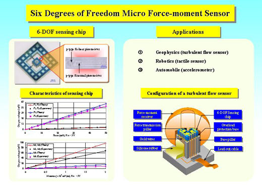
The
sensing chip is a crossbeam with piezoresistors on the upper surface.
The test particle has a diameter of 8mm and is made of polyethylene.
Its centroid will coincide with the center of the surface of the
crossbeam to minimize the moment induced by horizontal force components.
Forces and/or moments acting on the test particle will be transmitted
to the sensing chip via a force transmission pillar placed at
the center of the sensing chip. |
| |
|
|
| |
|
|
| |
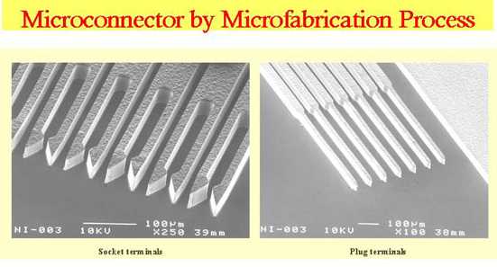
|
This
study focuses on fabrication of micro connectors by combining
UV thick resist photolithography and Ni electroforming. This fabrication
method is expected to realize high precision micro connectors
and high packaging density in mass production.
A
fork-type micro connector with high aspect ratio and high packaging
density was fabricated using UV thick photoresist and Ni electroforming.
A negative photoresist (THB-130N) was used as a mold of Ni electroforming.
The tips of socket terminal of the micro connector were formed
as movable portions using Cu sacrificial layer etching. In order
to make firm contact of the micro connector, two-step guidance
was adopted. The size of the terminal of fabricated micro connector
was 50 mm- thickness and 15 mm-width (minimum). The maximum aspect
ratio of the fabricated micro connector is 3.3 and the terminal
pitch is 80 mm. Figure 1 shows SEM photograph of the socket terminal
which was formed by the Ni electroforming. A contact resistance
of a 50 mW,a contact force of 2.08mN,Young痴 modulus of 80 GPa
and a permissible current of 400 mA (single pair of the plug and
socket terminals) were obtained practicl use for the micro connector.
|
| |
|
|
| |
|
|
| |
A new method of using silicon microneedle array in Bio-Medical
applications is introduced in this work. The hollow microneedle
array with the facilitation of an insertion guide array have been
designed and fabricated. The needles can be pushed down through
the second layer of human skin with less-bending. The tip of microneedle
will be led by the insertion guide to pierce the skin perpendicularly.
The silicon bulk micromachining technique using an inductively
coupled plasma (ICP) etcher has been employed to fabricate the
microneedle array and the insertion guide array. The array chips
are 5x5 mm2 for both structures. The needle array chip contains
100 microneedles with 100um and 30um of the outer diameter and
the hole diameter respectively. The guide array chip is 100 um-thick
and contains 100 guiding holes with 120 um diameter. A buckling
test of microneedle gave the result that there was no microneedle
broken during the test via the guiding holes. Contrary, there
were several microneedles broken during the penetration without
the facilitation of the guide.
|
 |
|
| |
|
|
| |
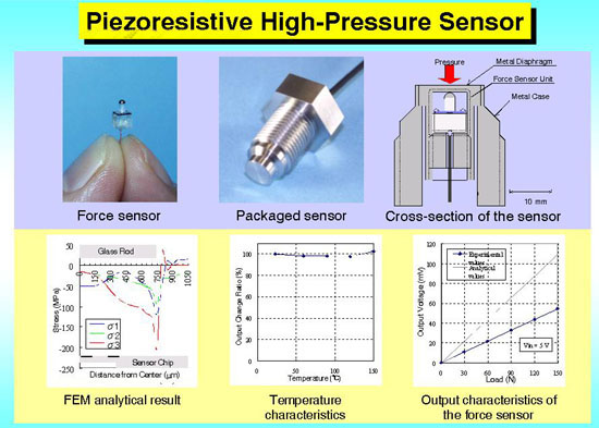
The
piezoresistive pressure sensor is reliable for precision pressure
measurement. In our Lab., a silicon piezoresistive pressure
sensor for high pressure measurement utilizing a combination
of three-axis stress components has been developed. The piezoresistive
pressure sensor can be used for measurement of internal pressure
in a injection molding machine. The pressure sensor was composed
of a force sensor, a stainless steel (SUS630) housing with a
diaphragm of 10 mm-diameter in which the force sensor was assembled,
a fix screw, a stainless steel (SUS630) case and a resin cap.
Pressure is transmitted into force which is applied to four
piezoresistors on a silicon sensor chip through a force transmission
rod of glass (SW-3). Stresses due to applied pressure in piezoresistors
depend on the diameter, height and Young's modulus of the rod,
and the diaphragm thickness of the sensor chip. In order to
obtain large resistance changes in piezoresistors, the optimum
combination of three-axis stress components was investigated
by changing of these parameters. An output of the prototyped
pressure sensor was more than 50 mV / 5 V at 150 MPa and a sensitivity
temperature characteristic was 0.11 % / centigrade in the range
from room temperature to 150 centigrade.
|
|
|
| |
|
|
| |
|
|
| |
SENSOR
NETWORK |
|
| |
|
|
| |
|
|
| |
|
|