STORY #3
Low-cost, high-efficiency, next-generation Thin-film Solar Cell to replace Silicon
Jakapan Chantana
Professor, Research Organization of Science and Technology
What would the structure of a thin-film solar cell that does not use harmful cadmium and yet achieves high photoelectric conversion efficiency look like?
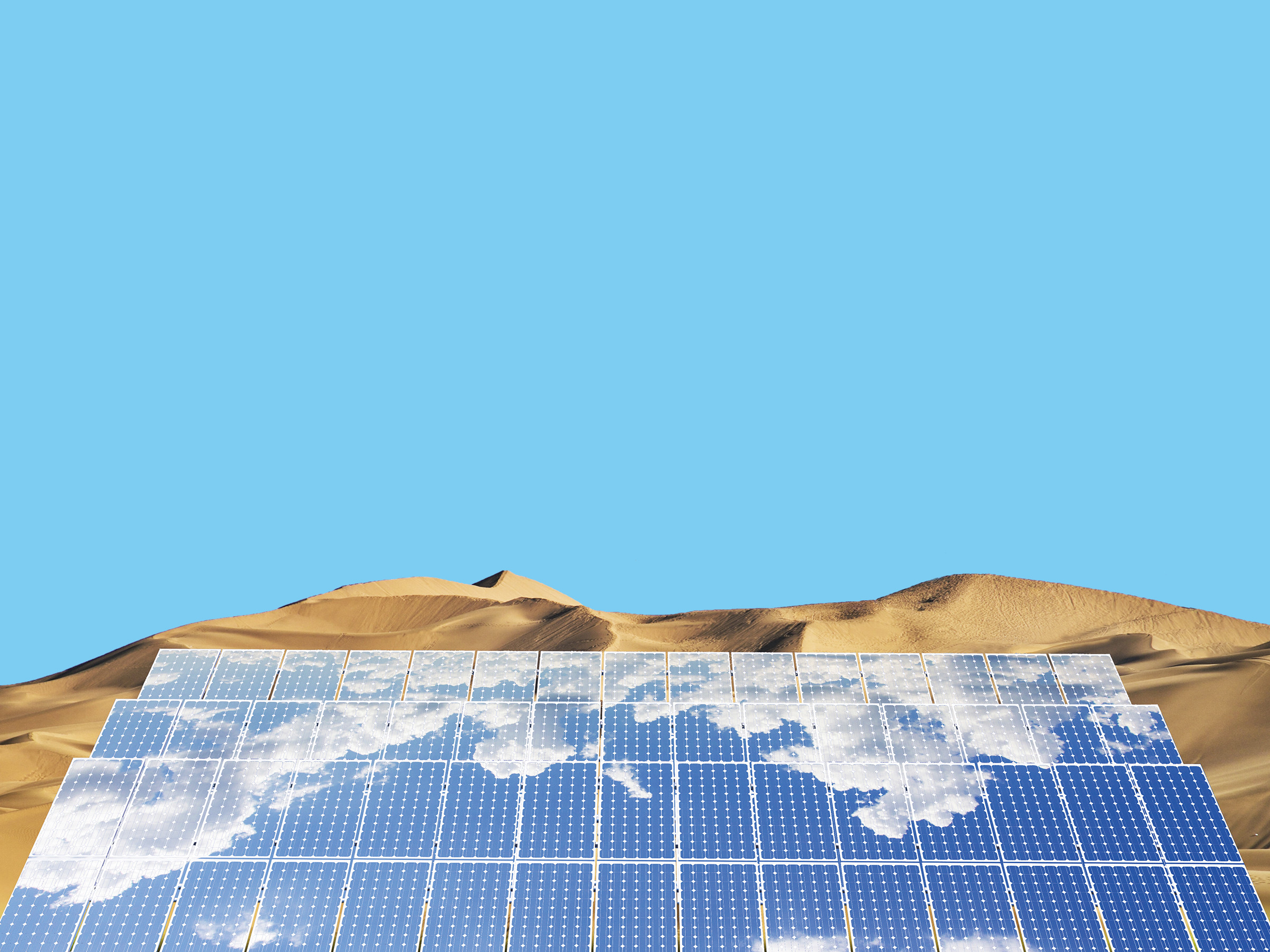
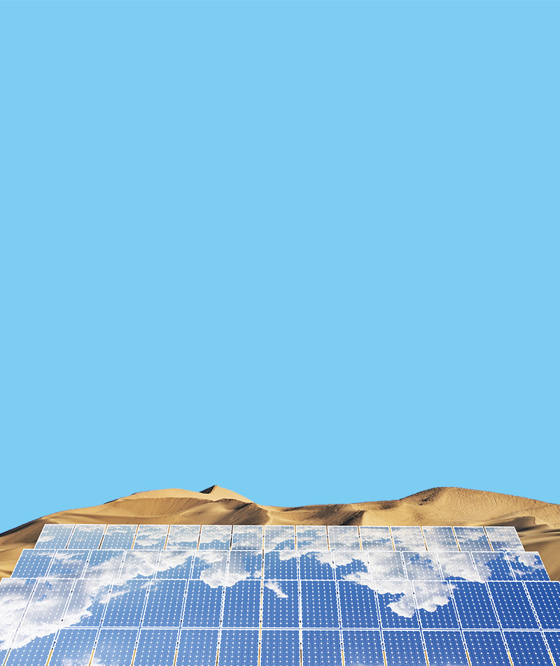
Today, as the number of energy-related problems, such as environmental pollution, the exhaustion of underground resources, natural disasters, and nuclear power plant accidents increases, renewable energy is becoming increasingly more important. In particular, expectations are high for solar power, but much development must take place before it can surpass existing power generation methods. Solar cells made from silicon currently have a market share of more than 90%, but there is a limit to the reductions in manufacturing costs that can be achieved; thus, significant efforts are being devoted to develop new types of solar cells that do not require silicon.
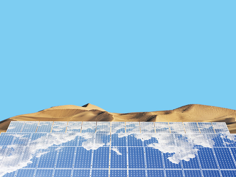
One such new kind of solar cell is the CIS thin-film solar cell, which mainly consists of copper (Cu), indium (In), and selenium (Se), with a chalcopyrite crystalline structure.
Jakapan Chantana is engaged in the development of solar cells that use Cu, In, Se, gallium (Ga), and sulfur (S), instead of silicon, for optical absorption.
CIS solar cells are characterized by their capacity to absorb about 100 times more light than silicon-based cells. They can also be made into thin films. The cell thickness of silicon solar cells is about 200 μm, while that of CIS thin-film solar cells is no more than 2–3 μm. This is the extent to which we hope to decrease resource use and costs. Yet, the photoelectric conversion efficiency of CIS thin-film solar cells remains inferior to that of silicon types, preventing replacement in the market.
Chantana explains, “The highest photoelectric conversion efficiency achieved for CIS thin-film solar cells in the world is 22%. These solar cells are still at the research stage. Nevertheless, there is still a big gap between this value and the 26.7% efficiency of silicon solar cells. In addition, CIS thin-film solar cells require rare metals such as cadmium and other materials that are toxic to the human body during the film deposition process. Furthermore, significant amounts of electricity are required to fabricate these high-quality thin films using a vacuum process.” To overcome these challenges, he is attempting to build highly efficient solar cells using a low cost, low power consumption method to fabricate the film while eliminating most of the expensive and hazardous materials.

The typical CIS thin-film solar cell has a substrate structure covered by rear-side electrodes, an optical absorption layer, a buffer layer, a window layer that lets light in, and a transparent conducting layer. There are several methods for creating these layers. Sputtering and other dry processes are used for the CIS optical absorption layer, while a wet process called solution growth is used for the deposition of the buffer layer between the CIS optical absorption layer and the transparent conducting layer. However, a wet process raises production costs, so it is preferable if all depositions can be achieved using dry processes. Another issue is that cadmium sulfide (CdS), a hazardous substance, is often used during the deposition of the buffer layer to achieve higher efficiency.
In recent studies, Chantana has created solar cells using different materials and deposition techniques for each layer to compare their photoelectric conversion efficiencies.
Chantana first fabricated a solar cell using a CIGSSe optical absorption layer and the conventional CdS wet process for the buffer layer (Fig.: Structure A). “We managed to achieve a photoelectric conversion efficiency of 18.3%, but we were left with the issue of a thick buffer layer that absorbs short-wavelength light.” To increase the efficiency, the buffer layers must be made thinner, or the short-wavelength photoelectric loss must be limited using a substance with a wide band gap.
Next, Chantana created a solar cell by substituting CdS with zinc sulfide (ZnS) and used sputtering to deposit a buffer layer (Fig.: Structure B). This resulted in a band gap of ZnS of 3.5 eV, which is wider than the 2.6 eV of CdS. This strategy eliminated the use of the harmful substance and reduced the short-wavelength photoelectric loss. Yet, Chantana explains, “Compared to the previous solar cell, the overall particle efficiency was low, and the voltage had clearly fallen.” The reason is that sputtering of the ZnO window layer that connects the buffer layer and the transparent conductive layer causes sputtering shocks, which damage the surface of the CIGSSe optical absorption layer. CdS is resilient against sputtering shock and protects the CIGSSe optical absorption layer from damage, but there was no substance to fulfill this shielding function in this new structure.
Therefore, Chantana decided to deposit a buffer layer that combines ZnS (O,OH) and an ultrathin CdS film to increase short-wavelength sensitivity while, at the same time, reducing the sputtering damage (Fig.: Structure C). As a result, short-wavelength sensitivity increased, and a high photoelectric conversion efficiency of 18.6% was achieved.
Furthermore, he succeeded in depositing all thin films using dry processes, employing a ZnMgO:Al transparent conductive layer and a ZnMgO buffer layer (Fig.: Structure D) to achieve a high photoelectric conversion efficiency of 20%. There is no known successful case in which a CIS thin-film solar cell was created using these materials. In his research so far, Chantana has developed a transparent conductive film that is able to control the conduction band positions, using thin films made of zinc (Zn), magnesium (Mg), or other ternary mixed crystals containing zinc. Mg has a wide band gap and lets in more light than conventional films that use only Zn, which is what enabled this high efficiency.
Chantana is confident, saying, “We can increase the photoelectric conversion efficiency further by changing the materials and deposition methods for each layer.” Chantana is leading the way in a highly competitive global race to develop CIS thin-film solar cell materials.
- Jakapan Chantana
- Professor, Research Organization of Science and Technology
- Subject of Research: Increasing the efficiency of CIS thin-film solar cells
- Research Keywords: Solar cells, solid-state electronics