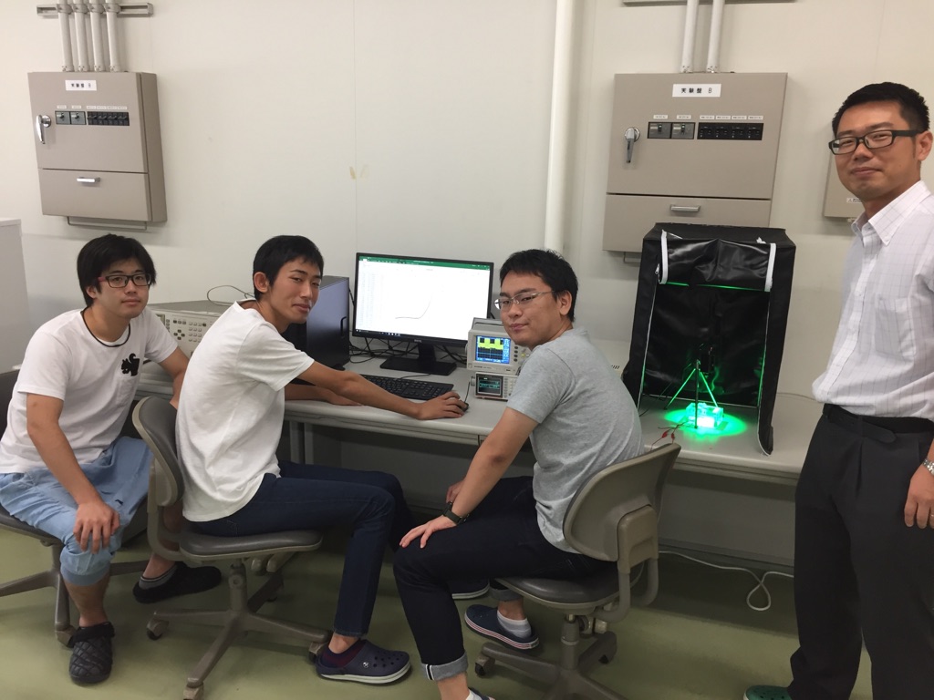
Advanced Functional Thin-Film Materials and Device Applications
Our laboratory conducts research on advanced manufacturing technologies that integrate light, electricity, and mechanics through the application of materials science. We focus on the development of functional thin-film materials and their applications in energy harvesting, sensing, photocatalysis, and neuromorphic devices. Current research topics include atomically thin materials such as graphene and MXenes, flexible piezophototronic photovoltaic devices, selenium-based indoor photovoltaics, photocatalytic thin films, and artificial synaptic devices for AI vision systems.
Atomically 2D Nanosheet and Their Applications (Graphene and MXenes)
Graphene consists of a single atomic layer of carbon atoms arranged in a hexagonal lattice. It is the thinnest material known on Earth and exhibits exceptional mechanical strength, flexibility, electrical conductivity, and optical transparency. Conventional transparent conductive materials, such as indium tin oxide (ITO), are widely used in optoelectronic devices including solar cells and light-emitting diodes. However, these inorganic materials are brittle and easily crack when bent, resulting in significant degradation of electrical conductivity. Graphene-based materials, in contrast, are flexible, mechanically robust, and electrically conductive. Flexible transparent conductive electrodes are particularly important for the realization of next-generation flexible optoelectronic devices. For example, solar cells require transparent conductive layers that simultaneously allow efficient light transmission and charge collection. Graphene-based hybrid electrodes provide an attractive alternative to conventional ITO electrodes. The figure below shows an example of a flexible transparent electrode consisting of stacked silver nanowires and graphene. Such materials can be freely bent while maintaining high electrical conductivity, making them promising for numerous flexible electronic applications.

Publications
[1] M. Akasaka, H. Kurokawa, T. Kobayashi*, "ZnMgO/Se Thin Film Photovoltaic Devices with Graphene/Silver Nanowire Stacked Flexible Transparent Conducting Electrodes", Physica Status Solidi A: Applications and Materials Science, accepted.
https://onlinelibrary.wiley.com/doi/epdf/10.1002/pssa.70402
[2] Yoshiki Kishima, Yushin Sawada, Kunal Jogendra Tiwari, Saiki Kitagawa and Taizo Kobayashi, "Fabrication and Characterization of MXene Electrodes for Se thin film photovoltaic devices", MRS Spring Meeting & Exhibit 2026, Apr 29, 2026, Poster presentation
Photovoltage Modulation by Mechanical Bending
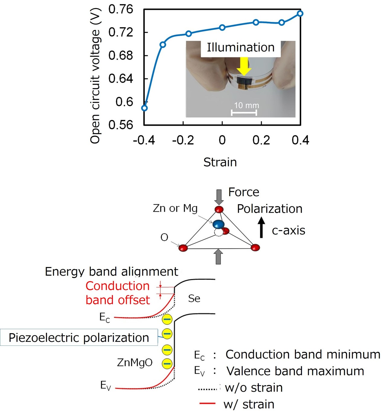
Solar Cells Whose Photovoltage Changes Upon Bending Our laboratory investigates flexible photovoltaic devices that exhibit changes in photovoltage when mechanically deformed by utilizing the piezophototronic effect, a coupling phenomenon among piezoelectricity, semiconductor physics, and photoexcitation. When tensile strain is applied to the device, photovoltaic performance is enhanced, whereas compressive strain reduces power generation. By controlling the direction and magnitude of bending, the open-circuit voltage can be continuously tuned. Unlike conventional strain gauges, which detect resistance changes and require external power supplies and bridge circuits, piezophototronic devices directly generate strain-dependent electrical signals. This characteristic enables self-powered strain sensing without external electrical excitation. The device employs a piezoelectric semiconductor layer based on ZnMgO. Mechanical deformation induces piezoelectric polarization charges within the ZnMgO layer, which modulate the interfacial barrier responsible for carrier transport and collection. As a result, the photovoltaic properties of the ZnMgO/Se heterojunction can be dynamically controlled through mechanical strain. Our group has successfully demonstrated flexible thin-film photovoltaic devices composed of ZnMgO-based window layers and crystalline selenium absorber layers fabricated on PET substrates. Significant strain-induced modulation of photovoltage has been observed.
Publications
[1] J. Fujimura, Y. Adachi, T. Takahashi and T. Kobayashi, "Impact of piezo-phototronic effect on ZnMgO/Se heterojunction photovoltaic devices" Nano Energy, Vol. 99, 107385 (2022)
[2] C. Tiange, R. Ogata and T. Kobayashi, "Piezophototronics effect of n-ZnMgO/p-Se hetero junction and its application to strain sensing", 37th International Microprocesses and Nanotechnology Conference (MNC 2024), 15. Nov. 2024
[3] Hiroya Kurokawa, Kosuke Nomura, Saiki Kitagawa, Taizo Kobayashi, "ZnMgO/Se Piezophototronic Device with Metal Grid Patterns/Graphene Stacked Flexible Transparent Conducting Electrodes", MRS Spring Meeting & Exhibit 2026, Apr 27, 2026, Oral presentation
Web news media 1("Japanese researchers investigating thin-film solar cells that react to indoor lighting", Renewable Energy Magazine)
Web news media 2 ("Thin-film flexible piezoelectric-photovoltaic cell based on selenium", PV Magazine)
Selenium Thin-Film Solar Cells for Indoor Energy Harvesting
Crystalline selenium is characterized by an extremely high optical absorption coefficient in the visible wavelength range, approximately 100 times greater than that of conventional silicon. The theoretical power conversion efficiency limit of a single-junction selenium solar cell under indoor illumination is expected to reach approximately 55%. Furthermore, selenium-based devices can be fabricated using relatively low-temperature processes below 200°C, enabling their integration onto polymer films. These characteristics make selenium an attractive material for lightweight and flexible photovoltaic devices designed to harvest energy from indoor lighting environments. Various energy-harvesting technologies utilizing indoor energy sources are being actively investigated for Internet of Things (IoT) applications. One of the key requirements for such technologies is that the power-generation device must be sufficiently inexpensive, lightweight, and compact compared with the target system it powers. Selenium thin-film photovoltaic devices consist of a simple multilayer structure fabricated from low-cost materials, making them promising candidates for a wide range of indoor energy-harvesting applications. Our research has focused on improving device performance through precise control of heterojunction interfaces, including investigations into stacked evaporation processes for accurate compositional engineering of the junction layers [1]. Interestingly, selenium was also the material used in the world's first solid-state solar cell. In 1883, the American inventor Charles Fritts developed the first solid-state photovoltaic device using a selenium layer sandwiched between thin, semi-transparent gold films. Selenium also played a central role in the discovery of photoconductivity by W. Smith in 1873 [2]. This research has been supported by research grants from the Amano Institute of Technology and the Ikeya Science and Technology Foundation in FY2024. We gratefully acknowledge their support. In addition to photovoltaic devices, our laboratory is engaged in the miniaturization and array integration of optical sensors by utilizing microfabrication technologies and the unique physical properties of thin films [3]. When a relatively low external voltage of approximately 3 V is applied to a selenium thin film, avalanche carrier multiplication can occur, resulting in highly sensitive photodiodes. Because of this property, crystalline selenium is considered a promising material for next-generation high-definition image sensors [4]. Moreover, selenium thin films can be deposited at relatively low temperatures (approximately 200°C), making them suitable for integration onto heterogeneous substrates and signal-processing chips. This research has been supported by JSPS KAKENHI Grant-in-Aid for Scientific Research (C) No. 18K04914, and we gratefully acknowledge this support.(Research introduction link)

Publications
[1] T. Kobayashi*, T. Miyamoto, R. Ogata, Z. Jehl Li Kao, “TiO2/Se heterojunction photovoltaic device made from Se/Te/Se stacked precursor”, Solar Energy Materials and Solar Cells, Vol.277, 113120 (9Pages), (2024)
[2] W. Smith, “Effect of Light on Selenium during the passage of an Electric Current” Nature(1873)
[3] Y. Adachi and T. Kobayashi*, "Formation of micro-patterned Ga2O3/Se heterojunction and its application to highly sensitive avalanche photodiode", Physica Status Solidi A: Applications and Materials Science ,Vol.220, Issue 5, 22006 (8 Pages) (2023).
[4] S. Imura et al., : “High-sensitivity image sensors overlaid with thin-film gallium oxide/crystalline selenium heterojunction photodiodes”, IEEE Trans. Electron Devices., Vol.63, No.1, pp.86-91 (2016)
Web news media 3 ("Japanese scientists build heterojunction solar cell based on titanium dioxide, selenium", PV Magazine)
Artificial Synaptic Devices for AI Vision Systems
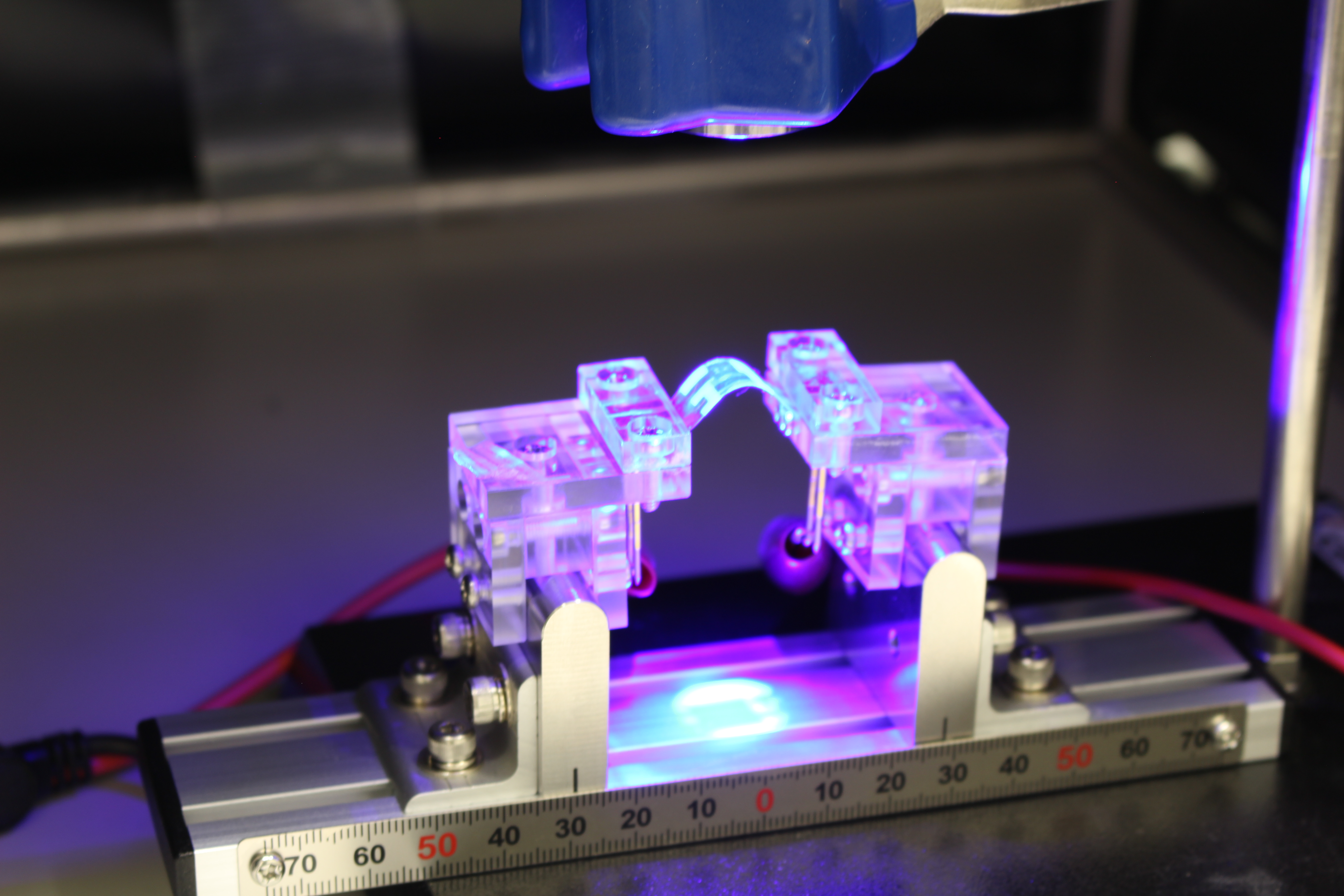
The human visual system recognizes images through highly efficient information processing, in which visual signals captured by the retina are transmitted and processed by the brain. This biological architecture enables rapid signal processing with remarkably low energy consumption. Inspired by this mechanism, neuromorphic vision systems that emulate the functions of the retina and brain have attracted considerable attention in recent years. To realize such systems, artificial synaptic devices are required to modulate and retain signal weights in response to optical stimuli. In particular, the transmission efficiency of signals should be strengthened in a non-volatile manner according to the intensity and frequency of incident light, analogous to synaptic plasticity in biological neural networks. Our previous studies on Cu(In,Ga)Se₂ (CIGS) thin-film solar cells and selenium (Se) thin-film photovoltaic devices have revealed that their performance can be modified non-volatilely through light-soaking treatments. This phenomenon originates from the light-soaking effect, in which the electrical states of defect levels within the semiconductor are temporarily altered by light exposure. As a result, photovoltaic performance can be persistently enhanced even after the optical stimulus is removed. By exploiting the similarity between this non-volatile photo-induced performance enhancement and biological synaptic plasticity, we are developing optically responsive artificial visual synapses based on selenium photovoltaic devices [1]. Our goal is to establish novel neuromorphic hardware that directly combines sensing, memory, and information processing functions within a single device structure. This research is supported by the JST FOREST Program (Fusion Oriented REsearch for disruptive Science and Technology, Grant No. JPMJFR246S). We gratefully acknowledge this support. International Collaborative Research Our laboratory also participates in international collaborative research projects in cooperation with European research institutions. Through these collaborations, we explore emerging concepts at the intersection of photovoltaics, piezophototronics, neuromorphic devices, and intelligent sensing technologies.
[1] Z. Jehl Li-Kao, K. Tiwari, S. Giraldo, M. Placidi, A. G. Medaille, A. Basak, E. Saucedo, T. Kobayashi "Investigating The Interplay of Piezoelectricity and Synaptic Plasticity in Se-Based Photodiodes for Optically Controlled Memristors on Flexible Substrates", 2024 MRS Spring Meeting, Seattle(USA), Apr 24, (2024)
Research on TiO₂ Photocatalytic Thin Films
Photocatalytic materials are promising functional materials for a wide range of applications, including zero-emission hydrogen production and biomedical technologies. Titanium dioxide (TiO₂), one of the most widely studied photocatalysts, exhibits various light-induced functionalities. Under ultraviolet irradiation, photogenerated charge carriers (electrons and holes) and reactive radicals generated within the TiO₂ film initiate a variety of surface reactions. For example, an increase in oxygen vacancies, which serve as adsorption sites for water molecules, can induce a highly hydrophilic surface state known as superhydrophilicity. In addition to wettability control, photocatalytic reactions enable several important applications. These include photocatalytic water splitting for the production of hydrogen and oxygen from water, as well as antimicrobial reactions that deactivate bacteria and viruses through the decomposition of their organic membranes. Our research focuses on developing novel high-performance photocatalytic thin films through comprehensive control of material properties and nanostructures. Specifically, we investigate methods for enhancing the localization of photogenerated carriers at the surface to improve photocatalytic activity and selectively control surface reactions. We also explore structural engineering approaches, including increasing surface area, optimizing chemical composition, and controlling crystalline structures to enhance overall photocatalytic performance. Research on photocatalytic wettability control has been supported by the JSPS Grant-in-Aid for Young Scientists (B), Grant No. 16K17505. Research related to photocatalytic hydrogen generation has been supported by the 37th Mazda Research Foundation Grant and the FY2024 Research and Development Grant from the Yashima Environment Technology Foundation. We gratefully acknowledge their support.
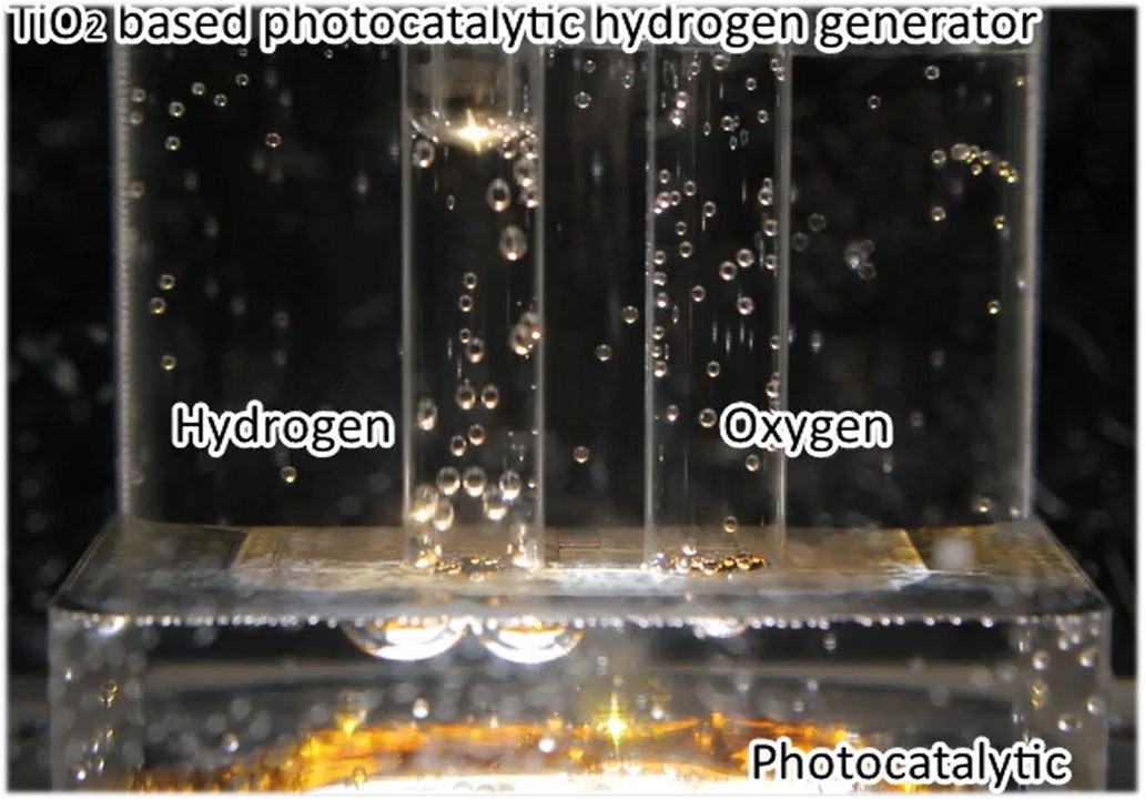
[1] K. Takatsuki, R. Takahashi and T. Kobayashi*, "Water-splitting Reactor Comprising a Combination of TiO2-based Photoelectrochemical Cell and Serially Connected TiO2/Se Heterojunction Photovoltaic Devices", Sensors and Materials,Vol.36, No.8(3), pp. 3367-3380 (2024)
Acknowledgements
Our research has been supported by the following competitive research grants and foundations. We gratefully acknowledge their support.
-Current project -
2025–2032 JST FOREST Program (Fusion Oriented REsearch for disruptive Science and Technology) Creation of Artificial Synaptic Functions Based on Piezophototronics Principal Investigator: Taizo Kobayashi
2024–2026 JSPS KAKENHI Grant-in-Aid for Scientific Research (B), Grant No. 24K01422 Mechanisms of Photovoltaic Performance Enhancement in Selenium-Based Photovoltaic Devices Using Mechanical Energy Principal Investigator: Taizo Kobayashi
FY2025 Iwatani Naoji Foundation Research Grant On-Chip Photocatalytic Reactor Integrating Water-Splitting Reactions and Hydrogen/Oxygen Bubble Collection Mechanisms Principal Investigator: Taizo Kobayashi
-Previous project-
2022–2023 JSPS KAKENHI Grant-in-Aid for Challenging Research (Exploratory), Grant No. 22K18797 Gigasecond Imaging Enabled by Pyramid-Shaped Photoconversion Layers Co-Investigator: Taizo Kobayashi Principal Investigator: Taeko Ando
2018–2020 JSPS KAKENHI Grant-in-Aid for Scientific Research (C), Grant No. 18K04914 High-Sensitivity Micro-Optical Sensors Based on Microfabricated Crystalline Selenium Heterojunctions Principal Investigator: Taizo Kobayashi
2016–2017 JSPS KAKENHI Grant-in-Aid for Young Scientists (B), Grant No. 16K17505 Development of High-Performance Wettability Switching Through Surface Structure and Carrier Control of Photocatalysts Principal Investigator: Taizo Kobayashi
2017–2019 JSPS KAKENHI Grant-in-Aid for Scientific Research (B), Grant No. 17H02091 Development of a Biohybrid System Incorporating Functional Devices for Cellular Metabolism Analysis Co-Investigator: Taizo Kobayashi Principal Investigator: Satoshi Konishi
Amano Institute of Technology Research Grant Development of Lightweight and Thin High-Efficiency Indoor Photovoltaic Devices Based on Selenium Thin Films Principal Investigator: Taizo Kobayashi FY2024
Iketani Science and Technology Foundation Research Grant Development of High-Quality Window Layers for High-Efficiency Indoor Photovoltaic Devices Based on Selenium Thin Films Principal Investigator: Taizo Kobayashi FY2024
Yashima Environment Technology Foundation Research and Development Grant On-Chip Photocatalytic Reactor with Vibration-Assisted Reaction Enhancement Mechanisms Principal Investigator: Taizo Kobayashi FY2023
Tateisi Science and Technology Foundation Research Grant A Lightweight and Flexible Piezophototronic Strain Sensors Based on Selenium Thin Films Principal Investigator: Taizo Kobayashi FY2022
Iketani Science and Technology Foundation Research Grant Performance Enhancement of Crystalline Selenium Photovoltaic Devices Through Graded Composition Engineering Principal Investigator: Taizo Kobayashi 2021–2022
37th Mazda Research Foundation Grant Highly Efficient Photocatalytic Hydrogen-Generating Microreactor Integrated with Indoor-Light-Sensitive Selenium Solar Cells Principal Investigator: Taizo Kobayashi