- Address: 1-1-1 Noji-Higashi, Kusatsu, Shiga
- e-mail: fujino@se.ritsumei.ac.jp
-
Department of VLSI System Design
College of Science and Engineering
Ritsumeikan University
- Member of IEEE
- Member of IEICE (The Institute of Electronics, Information and Communication Engineers)
- Member of JSAP (The Japan
Society of Applied Physics)
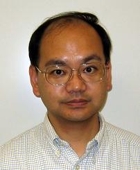
Takeshi Fujino was born in Osaka, Japan, on March 17, 1962. He received
B.S. and M.S., and Dr. degrees in electronic engineering from Kyoto
University, Kyoto, Japan, in 1984, 1986, and 1994, respectively. He
joined the LSI Research and Development center, Mitsubishi Electric
Corp. in 1986. Since then, he had been engaged in the development of
electron beam lithography process, and embedded DRAM circuit design. In
2003, he moved to Ritsumeikan University, Shiga, Japan, and
currently he is a professor of department of electric and electronic
engineering. His research interests include high-performance LSIs with
large-scale embedded memory, and its' applications for network system.
List of Papers
Go to
List of Papers page.


